Custom Components

Hunan Guoci New Material Technology Co., Ltd.

Alumina Ceramic Parts,Semiconductor Ceramic Parts
Alumina Ceramic Electrostatic Chucks
Alumina Vacuum Chucks
Alumina Ceramic Semiconductor Electrostatic Chucks
Alumina Ceramic Photovoltaic Chucks

Alumina Ceramic Electrostatic Chucks Alumina Vacuum Chucks Custom Ceramic Semiconductor Electrostatic Chucks


Material: Aluminum Oxide, Alumina, 95%-99.9% Al₂O₃

Sizes:Min-OD: 0.02mm; Max-length: 500mm

Customized: Can be custom for special sizes and shapes

Delivery Times:2 -25 days(depends on the structure and quantity)

Features:High hardness, Wear resistance, High temperature insulation, High dielectric strength, High mechanical strength.

  1. Fracture Toughness (MPa·m¹/²): 3.8-4.4
  2. Refractoriness: 1500-1750℃
  3. Density: 3.7-3.95g/cm3
  4. Flexural Strength (MPa): 300-375
  5. Thermal Conductivity: 25-30W/M.K
Transport Package: Cartons, Wooden Box

Shipment: by sea by air by courier by post etc.

    Welcome to leave us a message

  • Close

Product Description

Alumina ceramic vacuum chucks are made of high-purity alumina (Al₂O₃, typically 95% or above) ceramic and feature numerous micropores on their surface, either flat or custom-shaped. These micropores, through vacuum pressure, hold workpieces (such as silicon wafers, glass substrates, and electronic components) in place for handling, positioning, processing, or inspection.

This essential fixture, particularly in high-end precision manufacturing, is particularly important in the semiconductor and display panel industries. It perfectly demonstrates how the properties of alumina ceramic materials can solve specific industrial challenges. Ultrasonic or laser processing is used to create a regularly arranged pattern of extremely fine pores on a dense alumina ceramic plate. This is the most common form, offering the highest precision and excellent controllability.

Performance and Advantages (Why Alumina Ceramic?)

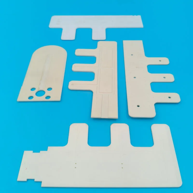
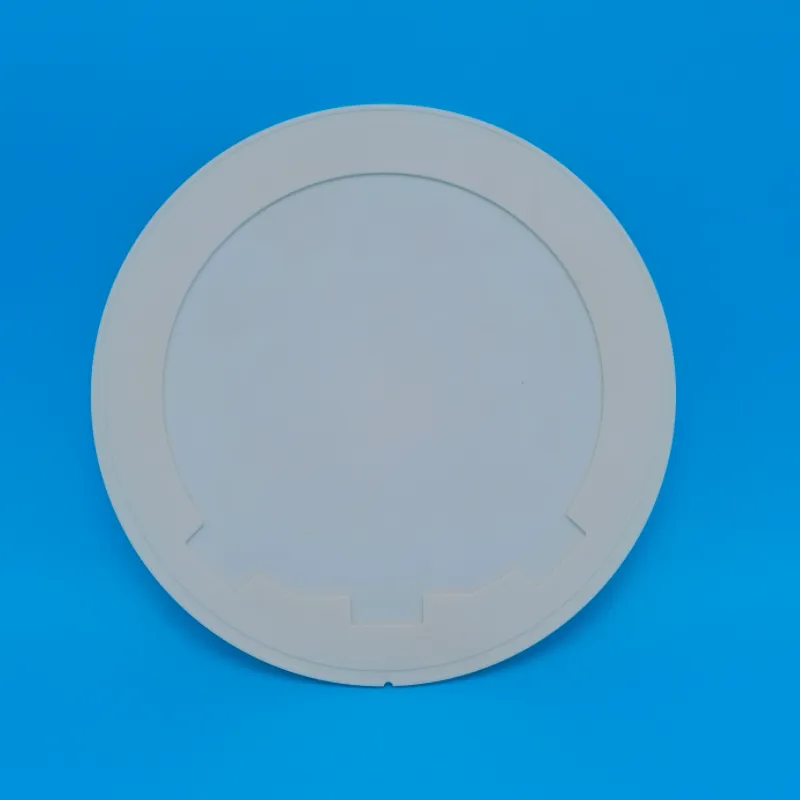
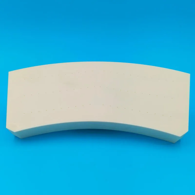
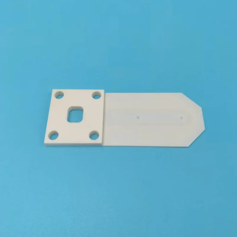
The material properties of alumina ceramic make it an ideal choice for vacuum chucks:

1. Extremely Hard and Flat:
With a Vickers hardness of > 1600 HV, it is extremely wear-resistant and not easily scratched by the workpiece. Ultra-high flatness down to the nanometer level (nm) can be achieved through precision grinding. This is crucial for processes like semiconductor lithography, as any surface irregularities on the chuck are directly replicated on the wafer.

2. Excellent High-Temperature Resistance:
It can withstand long-term operating temperatures up to 1500°C. This means it can be used directly in processes requiring heat, such as semiconductor thin film deposition (CVD/PVD) and etching, without deformation or degradation.

3. Excellent Chemical Stability:
It is resistant to strong acids, strong bases, and various organic solvents, and will never rust. It can withstand the frequent and harsh cleaning processes (including plasma cleaning) used in semiconductor manufacturing, ensuring an extremely long lifespan.

4. Extremely Low Contamination (High Purity):
High-purity alumina ceramic emits virtually no metal ions or particulate contaminants. This is essential for the semiconductor and optical industries, where cleanliness is paramount, preventing product contamination.

5. Excellent Thermal Performance:
  • It has a low coefficient of thermal expansion and excellent thermal stability, maintaining dimensional stability during thermal cycling and ensuring positioning accuracy. 
  • Heaters or cooling channels can be integrated according to the design to achieve precise control of workpiece temperature.

6. Customizable Porous Structure:
Through precision machining or molding processes, adsorption pores with pore sizes ranging from a few microns to several hundred microns can be created to accommodate workpieces of varying weights, sizes, and surface characteristics.

Main Application Areas

Alumina ceramic vacuum chucks are core fixtures in the following high-tech manufacturing industries:
1. Semiconductor Manufacturing (the most critical application)
  • Photolithography machines (steppers/scanners): Used to hold and secure silicon wafers, they require extremely high flatness and stability (to prevent nanometer-level jitter). 
  • Thin-film deposition (CVD/PVD), ion implantation, and etching: Used within the reaction chambers of these devices to hold and often heat wafers to achieve uniform process results.
  • Chemical mechanical polishing (CMP): Used to hold wafers for polishing.

2. Flat-panel display (FPD) manufacturing: Used to hold and transfer large, thin, and fragile workpieces such as glass substrates and OLED panels.

3. Precision electronics assembly: Used in SMT placement machines, die bonding, and other equipment to hold and precisely position PCBs, small ceramic substrates, or bare chips.

4. Optical and laser processing: Used to hold workpieces such as lenses, prisms, and wafers for cutting, grinding, and coating.